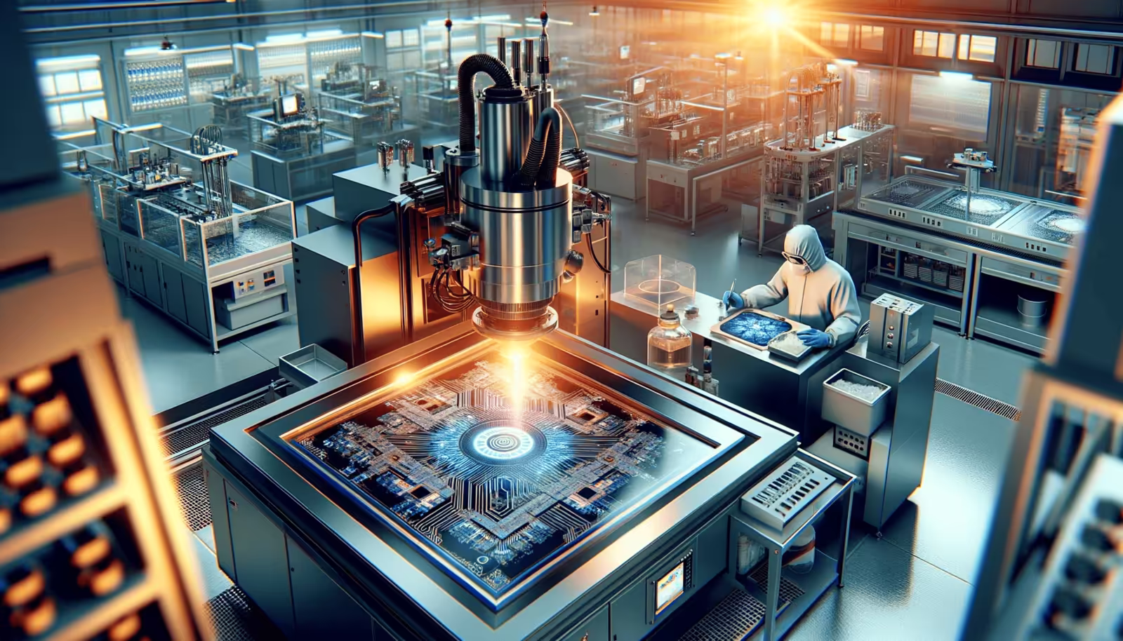
Plasma etching is a foundational technology in modern electronics manufacturing, enabling the precision and versatility needed to produce high-performance electronic components.
By leveraging the power of ionized gases, plasma etching plays a critical role in processes such as UV ozone cleaning, photoresist removal, PCB desmearing, wire bonding preparation, and substrate treatment.
This blog explores the intricacies of plasma etching, its diverse applications across industries, and how SCI Automation's innovations elevate the process to meet the demands of today's advanced technologies.
What is Plasma Etching?
Plasma etching is a process that uses ionized gas, or plasma, to precisely remove material from a surface.
This method involves controlling the composition of the plasma and its etching conditions to achieve high precision and clean results. It is instrumental in creating intricate patterns and structures on materials such as semiconductors, printed circuit boards (PCBs), and other electronic devices.
The precision of plasma etching is particularly vital in enabling the miniaturization of electronic components.
By removing material layer by layer at the microscopic level, manufacturers can achieve compact designs without compromising functionality.
Additionally, plasma etching's ability to modify surfaces without damaging the underlying material makes it indispensable for industries requiring exacting standards of quality and performance.
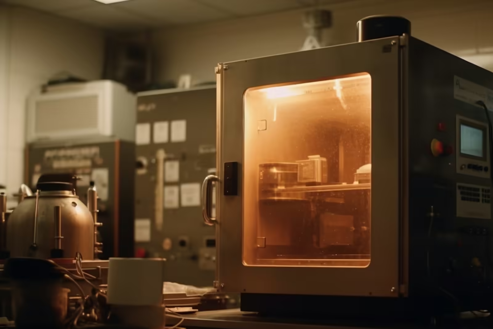
How Plasma Etching Works
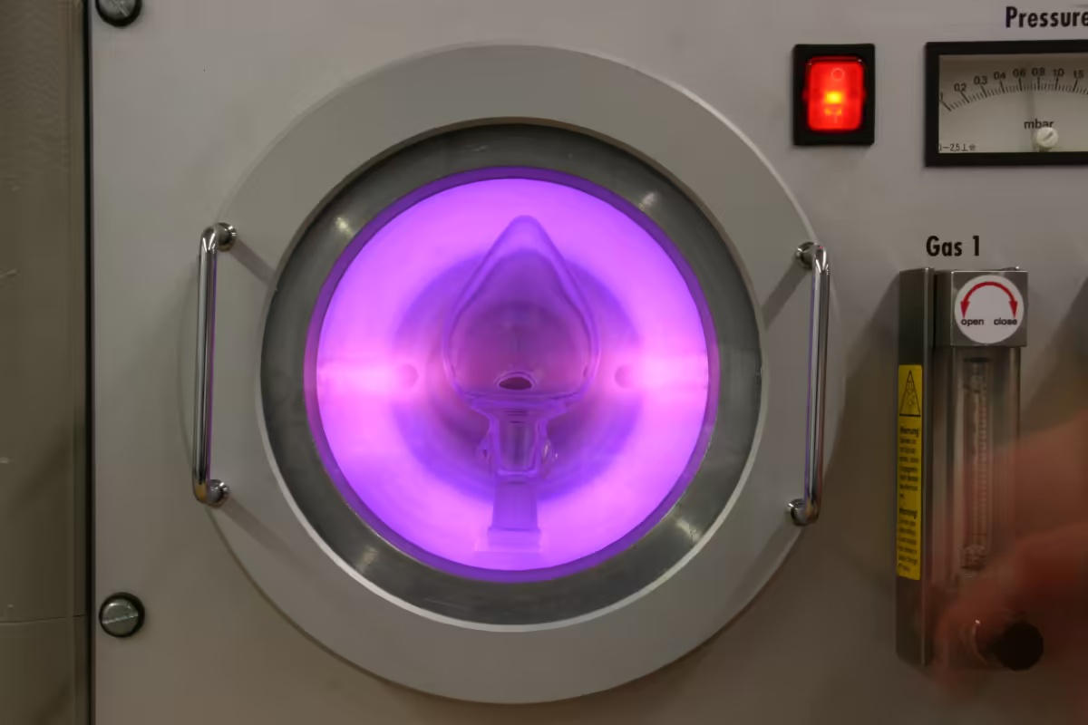
At its core, plasma etching relies on the generation of plasma - an energized state of matter composed of ions, electrons, and neutral particles.
By exposing a material to this plasma in a controlled environment, the process selectively removes material through chemical reactions and physical bombardment.
The specific type of plasma etching used depends on the application, with methods like Reactive Ion Etching (RIE), Inductively Coupled Plasma Reactive Ion Etching (ICP-RIE), and Deep Reactive Ion Etching (DRIE) offering varying levels of precision and efficiency.

Key Types of Plasma Etching
There are several types of plasma etching that it's important to be aware of.
Here are some of the most popular ones.
Reactive Ion Etching (RIE)
RIE combines chemical reactions and ion bombardment to remove material with high precision. By controlling the directionality of the ions, RIE achieves anisotropic etching, where material removal occurs primarily in one direction.
This technique is widely used for creating sharp, well-defined features in semiconductor devices.
For instance, RIE is critical in manufacturing microelectromechanical systems (MEMS), where intricate patterns on silicon wafers are essential for functionality. Its ability to produce precise, repeatable results has made it a cornerstone of semiconductor fabrication.
Inductively Coupled Plasma Reactive Ion Etching (ICP-RIE)
ICP-RIE builds on the principles of RIE by introducing a higher-density plasma and decoupling the ion acceleration and plasma generation processes.
This allows for better control over etching parameters, enabling higher etch rates and improved uniformity.
ICP-RIE is ideal for applications requiring deep, precise etching of hard materials like glass and ceramics.
Advanced semiconductor manufacturers often use ICP-RIE to produce high-frequency RF components and other complex devices. Its versatility and precision make it indispensable for cutting-edge technologies.
Deep Reactive Ion Etching (DRIE)
DRIE is a specialized method for creating deep, high-aspect-ratio features.
It is most commonly used in through-silicon vias (TSVs) for 3D integrated circuits and in MEMS devices requiring deep etches.
DRIE's ability to achieve extreme precision makes it the preferred choice for fabricating advanced silicon-based structures.
Plasma Ashing
Plasma ashing, also known as dry stripping, is used to remove photoresist and other organic materials following lithography processes.
This technique ensures thorough cleaning without damaging underlying structures, a critical requirement in semiconductor manufacturing and microfabrication.
Applications Across Industries
Plasma etching can be seen across a range of industries, including semiconductor manufacturing, medical devices, and more.
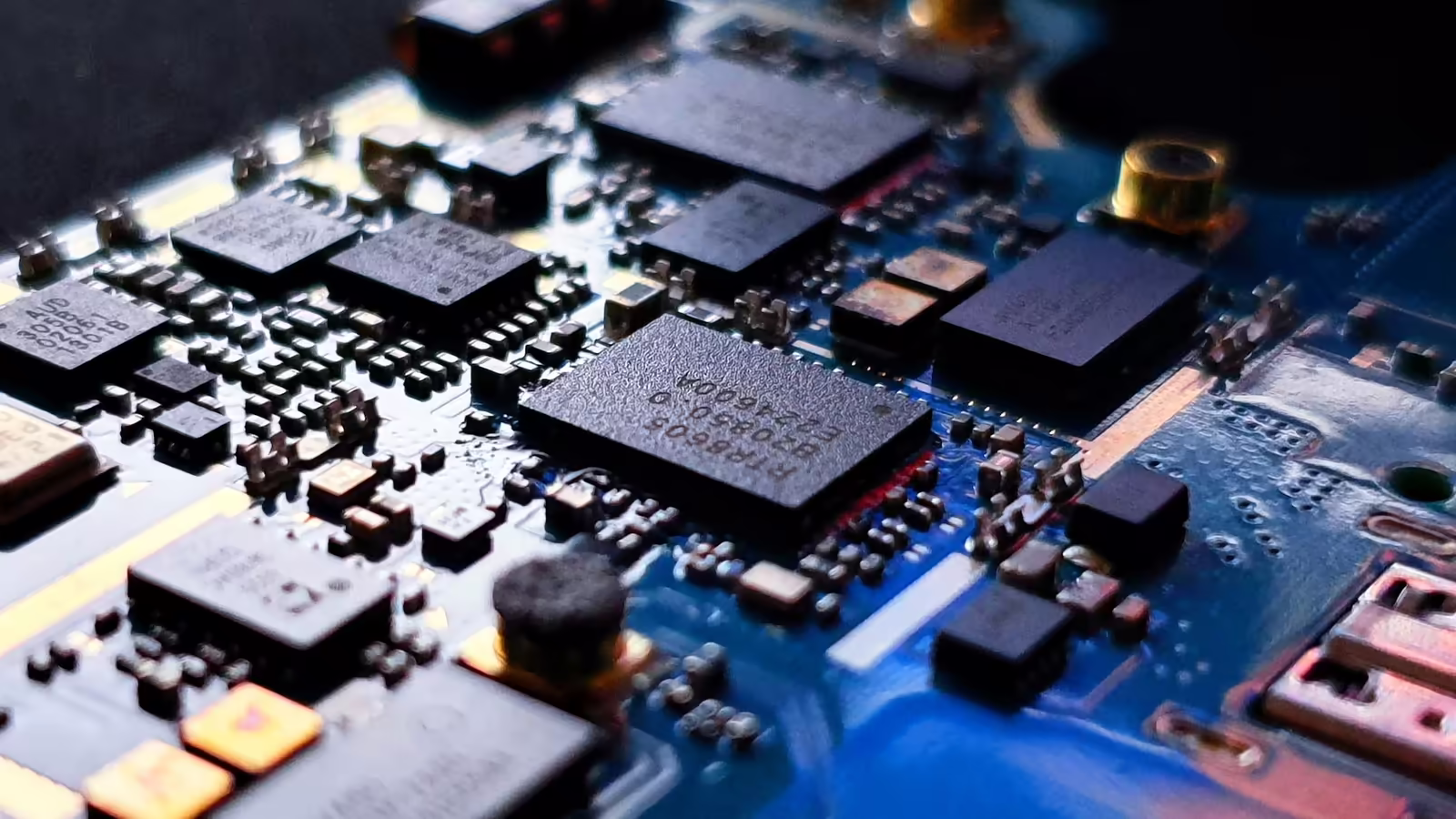
Semiconductor Manufacturing
Plasma etching is a cornerstone of semiconductor fabrication, enabling the creation of nanoscale features that drive the functionality of modern electronic devices.
From transistors to memory chips, plasma etching ensures the precision needed to produce increasingly compact and complex devices.
A practical example includes the use of ICP-RIE to achieve intricate patterns on silicon wafers for next-generation microprocessors. These advancements enable faster processing speeds and reduced power consumption, addressing the growing demand for energy-efficient electronics.
Medical Devices
In the medical field, plasma etching is vital for modifying the surfaces of implants and devices. By tailoring surface properties, manufacturers can improve biocompatibility and adhesion, ensuring the safety and reliability of critical components.
For example, plasma etching is often used to prepare titanium implants, enhancing their integration with human tissue.
This reduces rejection rates and improves patient outcomes, highlighting the importance of precision surface treatments in healthcare.
Aerospace and Defense
The aerospace industry benefits from plasma etching for treating advanced materials like composites and ceramics.
These treatments improve adhesion for protective coatings and enhance the durability of components operating in extreme environments.
In one instance, plasma etching was used to prepare composite materials for adhesive bonding in aircraft manufacturing, resulting in stronger, more reliable joints that meet stringent safety standards.
Technical Insights
The effectiveness of plasma etching depends on several technical parameters, including etch rates, precision levels, and material compatibility.
Plasma etching offers etch rates ranging from nanometers per minute for highly controlled processes to several micrometers per minute for rapid material removal. Advanced methods like ICP-RIE and DRIE deliver sub-nanometer precision, allowing for the creation of intricate structures with minimal material waste.
Material compatibility is another key advantage. Plasma etching can process a wide range of materials, including silicon, polymers, metals, and ceramics.
By selecting the appropriate gas - such as oxygen, fluorine, or argon - manufacturers can customize the process to achieve desired results for specific applications.
Real-World Applications
Now that you're aware of what plasma etching is and how it's used across industries, you may be wondering about some of its real-life applications.
Here are a few examples:
- UV Ozone Cleaning - This process combines ultraviolet light and ozone gas to clean delicate electronic components and semiconductors. It provides a chemical-free, highly effective cleaning solution.
- PCB Desmearing - Plasma etching removes epoxy and glass smears from drilled vias in PCBs, ensuring strong electrical connections and reliable performance in electronic devices.
- Wire Bonding Preparation - By cleaning and texturizing bonding surfaces, plasma etching enhances the adhesion and conductivity of wire bonds, ensuring long-term reliability in semiconductor devices.
- Substrate Treatment - Plasma etching modifies the surface properties of substrates, improving adhesion and enabling advanced functionalities in compact electronic components.
Why Partner with SCI Automation?
SCI Automation brings decades of expertise to the field of plasma technologies. Our innovative solutions are tailored to meet the unique needs of industries ranging from semiconductors to aerospace.
With cutting-edge equipment and a commitment to quality, we help clients achieve exceptional precision and efficiency in their manufacturing processes.
If you're looking to elevate your production capabilities with advanced plasma etching systems, contact SCI Automation today.
Whether you need tailored RIE solutions or customized substrate preparation, we're here to help you drive innovation and achieve excellence.