

Plasma Ashing for Photoresist Removal
Photoresist that isn't fully cleared doesn't look dirty. It shows up a process step or two later as a defect nobody traces back to the resist.
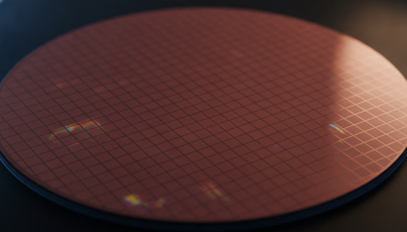
Photoresist is a temporary mask: applied to a wafer, patterned by lithography, and used to protect specific areas during etching or ion implantation. Once that step is done, the resist has done its job and has to come off completely before the wafer moves on — a trace left behind doesn't just look untidy, it interferes with the next process step, whatever that step happens to be. Getting that removal complete without damaging the pattern or the substrate underneath is what plasma ashing is built to do.
Why leftover resist threatens the next process step
Photoresist is a temporary structuring layer, not a permanent one, and every subsequent step in the process — metal deposition, further lithography, wafer-level packaging, flip-chip bonding — assumes it's gone. A residue that survives removal sits on the wafer as contamination, and because these residues are typically on the nanometre scale, they're invisible to the naked eye while still being large enough to interfere with the uniformity of whatever comes next: deposited metal that doesn't adhere consistently, or an interconnect that doesn't form the same way across a wafer that looked clean under normal inspection. The failure isn't in the equipment running the next step; it's in resist removal that wasn't as complete as it looked.
How oxygen plasma ashing removes photoresist
Oxygen plasma ashing ionises oxygen gas into a mix of reactive ions and radicals that chemically attack the photoresist — a carbon-based, organic material — breaking it down into simple, volatile byproducts like carbon dioxide and water vapour that are pumped out of the chamber, rather than mechanically stripped or dissolved off the wafer. Reactive-ion etching (RIE) is one common way of running this: it combines physical sputtering from ion bombardment with the chemical reaction from radicals, which makes it fast and effective, but the same energetic ions that make it effective can also physically damage a sensitive underlying layer if the process isn't controlled carefully. Getting that control right means monitoring plasma power, gas flow rate and chamber pressure throughout the cycle, so the process stays inside the window where the resist clears completely without the ion energy carrying over into the substrate.
Dry ashing versus gentler removal routes
The same precision-versus-throughput trade-off that runs through etching generally applies to resist removal. A dry, plasma-based process gives fine control over how aggressively material is removed and where — valuable as feature sizes shrink and the margin for substrate damage shrinks with them. Gentler dry alternatives, like UV-Ozone ashing, trade some of that speed for an even lower risk of ion-driven damage on layers that can't tolerate it. Which approach fits depends on how damage-sensitive the layer underneath the resist is, and how much throughput the line needs.
Where photoresist ashing sits in the process
Ashing is introduced immediately after the etch or implant step the resist was protecting, before the wafer moves on to the next deposition or lithography stage. It isn't unique to front-end wafer processing either — flip-chip bonding and wafer-level packaging both use photoresist for patterning, and both need it fully cleared before the next assembly step. The right system depends on the substrate and how much plasma energy the resist needs to clear:
- Aeon-HP — a high-power batch system with integrated temperature monitoring and heat dissipation for sustained plasma etching on organic surfaces, suited to resist that needs more energy or more dwell time to clear completely than a standard-power cycle delivers.

Verification
A completed ashing cycle should be checked for two things: that the organic residue is actually gone, and that the substrate underneath wasn't damaged getting there. Monitoring plasma power, gas flow and chamber pressure during the cycle catches process drift before it shows up as an incomplete or overly aggressive ash; inspecting the cleared surface afterward — a post-ashing analysis — confirms the cycle actually delivered what the monitoring data said it should have.
Recommended systems
Related industries
Related articles
Oxygen Plasma Ashing: Precision Sample Preparation
Oxygen plasma ashing is like a high-tech cleaning service for microscopic surfaces. Imagine you have a delicate piece of art covered in...
Photoresist Removal: Essential Processes in Microfabrication
See how the essential photoresist removal processes is crucial for precision and efficiency in modern microfabrication.

Dry Etching vs Wet Etching: Choosing the Right Method
As a fundamental step in the fabrication of semiconductors, etching involves the selective removal of material layers to craft these...
Frequently asked questions
Why does leftover photoresist matter if it's too thin to see?
Even nanoscale residue interferes with whatever comes next — deposited metal that doesn't adhere consistently, or an interconnect that doesn't form uniformly across the wafer. The defect isn't in the next process step's equipment; it's in resist removal that wasn't as complete as it looked.
How does oxygen plasma ashing actually remove photoresist?
Oxygen gas is ionised into reactive ions and radicals that chemically break the photoresist — a carbon-based material — down into volatile byproducts like carbon dioxide and water vapour, which are pumped out of the chamber rather than mechanically stripped off the wafer.
Is RIE-based ashing safe for every layer?
Not automatically. RIE combines physical ion sputtering with chemical reaction, which makes it fast and effective, but the same energetic ions can damage a sensitive underlying layer if the process isn't tightly controlled. Gentler dry methods trade some speed for lower damage risk on layers that can't tolerate it.
Is photoresist ashing only used in front-end wafer fabrication?
No. Flip-chip bonding and wafer-level packaging also use photoresist for patterning, and both need it fully cleared before the next assembly step.
Which plasma system fits a photoresist-ashing step?
Aeon-HP is the fit: a high-power batch system with integrated temperature monitoring and heat dissipation, built for sustained plasma etching on organic surfaces where the resist needs more energy or dwell time to clear completely than a standard-power cycle delivers.