

Technology &
Plasma Insights
Articles on plasma cleaning, surface treatment, and semiconductor manufacturing from the SCI Plasma engineering team.
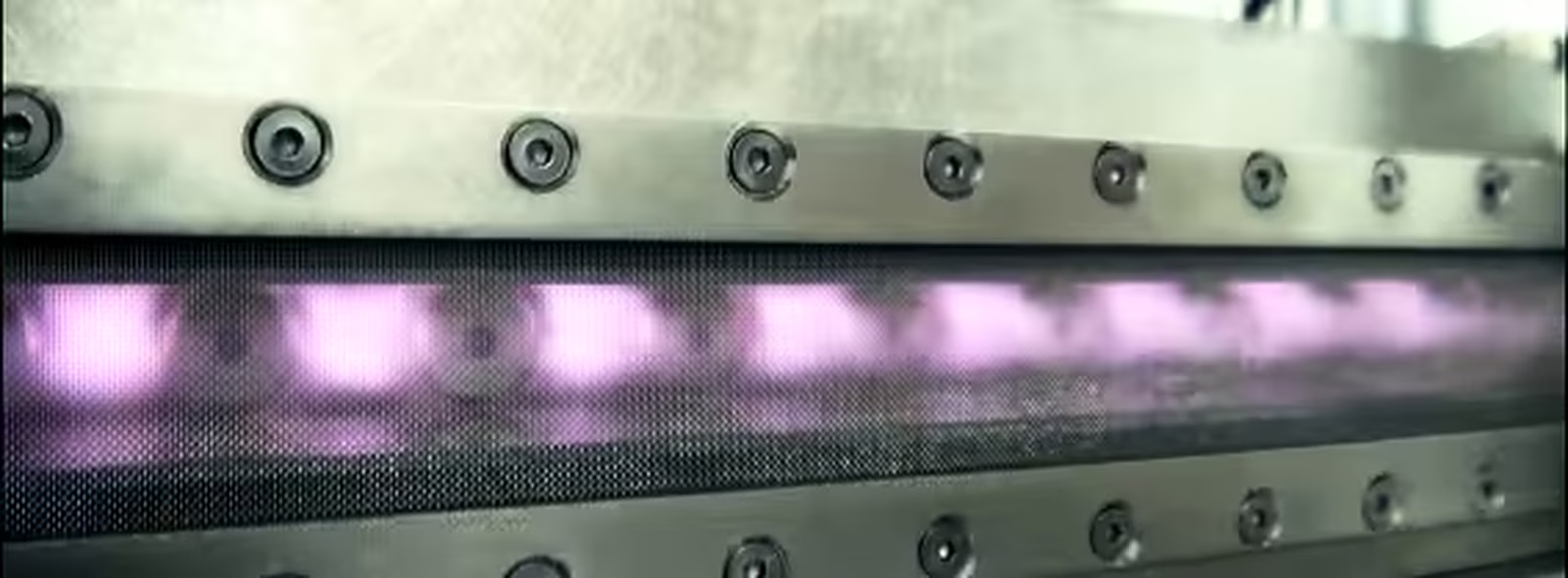
Semiconductor Plasma Cleaning: How the Process Works and Where It's Used
Semiconductor manufacturing leaves little room for surface contamination. This guide explains how plasma cleaning works, where it is used in assembly and packaging, how it helps prevent NSOP, and which plasma system options suit semiconductor production.
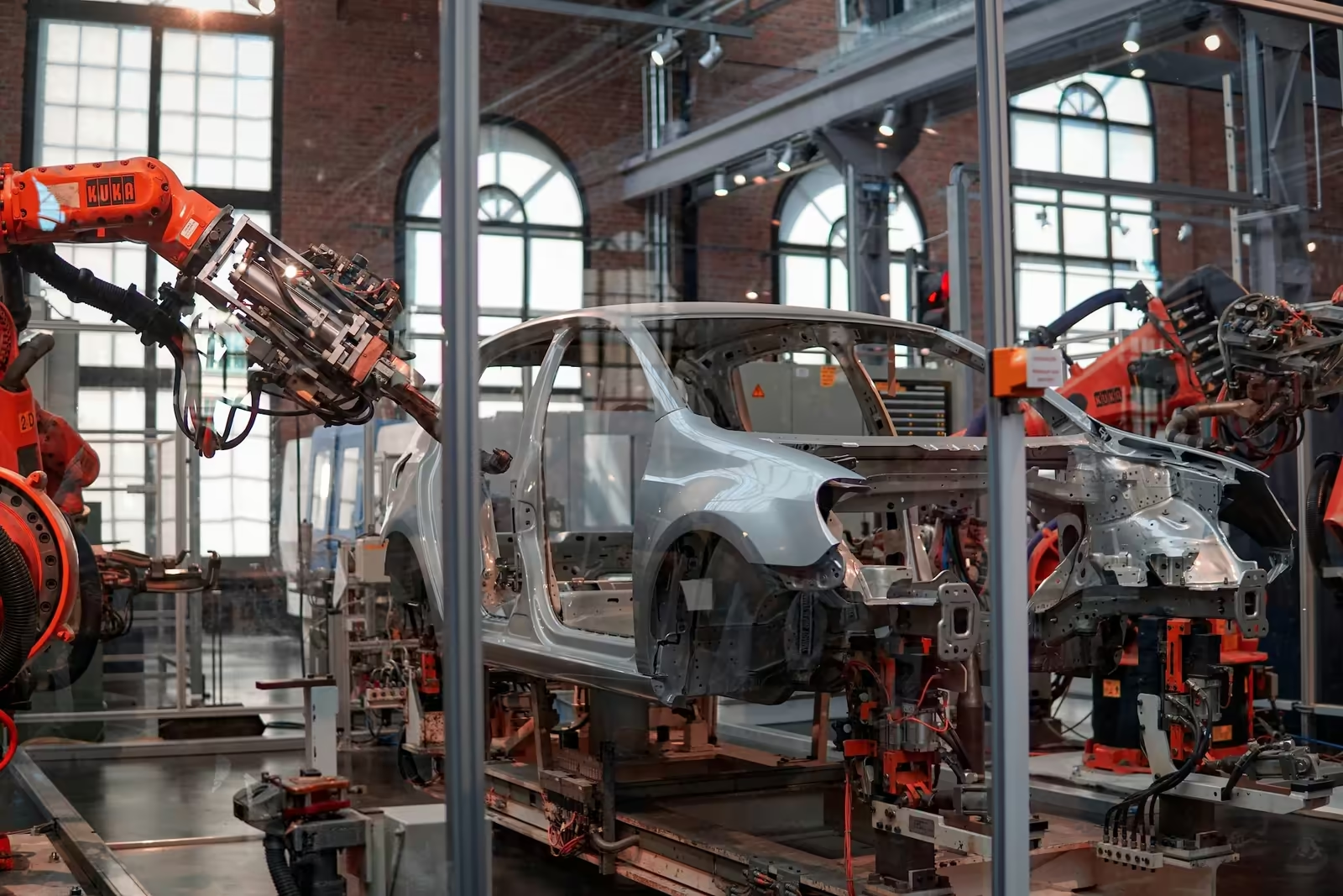
Atmospheric Plasma Cleaning: Solving Surface Contamination and Adhesion Problems in Manufacturing
In high-performance manufacturing, small surface variations can have a big impact on final product quality.
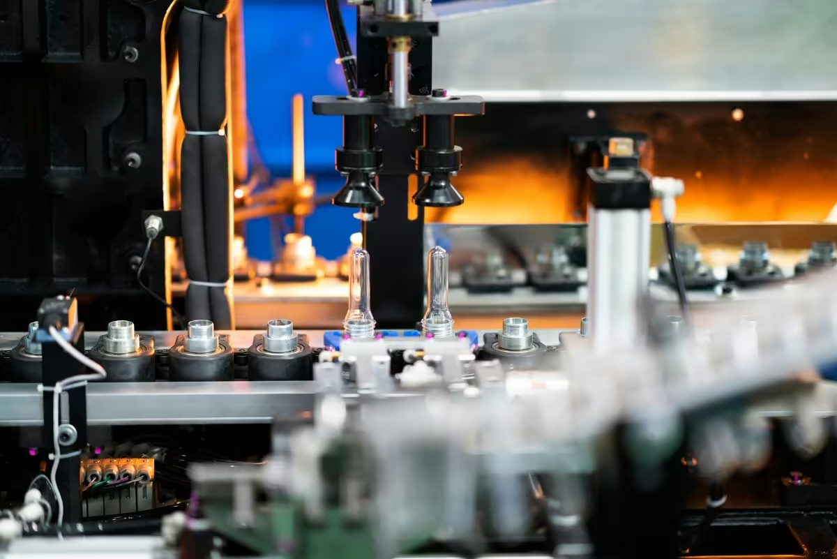
Improving Manufacturing Throughput Without Compromising Quality
Understanding what is truly restricting throughput is the first step toward solving it and unlocking a more reliable, high-yield production process.
Why Your Wire Bonding Is Failing and How to Fix It with Plasma Cleaning
Wire bonding failures don't happen by accident, and blaming machines or operators misses the real problem.
Plasma Cleaning Explained: What It Does and Why It Matters for Adhesion
Discover plasma cleaning, an eco-friendly, cost-effective way to remove unwanted materials from object surfaces. Learn how it works here.

Batch vs Inline Cleaning Equipment: Which Treatment Solution is Right For Each Production Line
In this guide, we explore how batch and inline systems works, where they are commonly used, and how to determine which option is best suited to your operation.
Bond Strength and Yield: Engineering Stability into Every Frame
Bond strength isn't a constant—it's the outcome of surface prep, material control, and the process environment. When failures occur,...

How Plasma Cleaning Solves Delamination Risks in Multi-Material Assemblies
When two materials don't bond properly, failure is often only a matter of time. Delamination—where bonded surfaces separate under stress...
Lead Frame Handling Challenges: How Complex Frames Affect Production
Warped or sagging lead frames turn automated handling into mispicks, jams and scrap. This guide covers how to engineer handling systems for real-world frame variability, and where vacuum plasma cleaning fits in the lead frame process.
Plasma-Assisted ALD: Precision for High-Tech Coatings
Atomic layer deposition (ALD) is a revolutionary thin-film coating technology that has become indispensable in industries where precision...
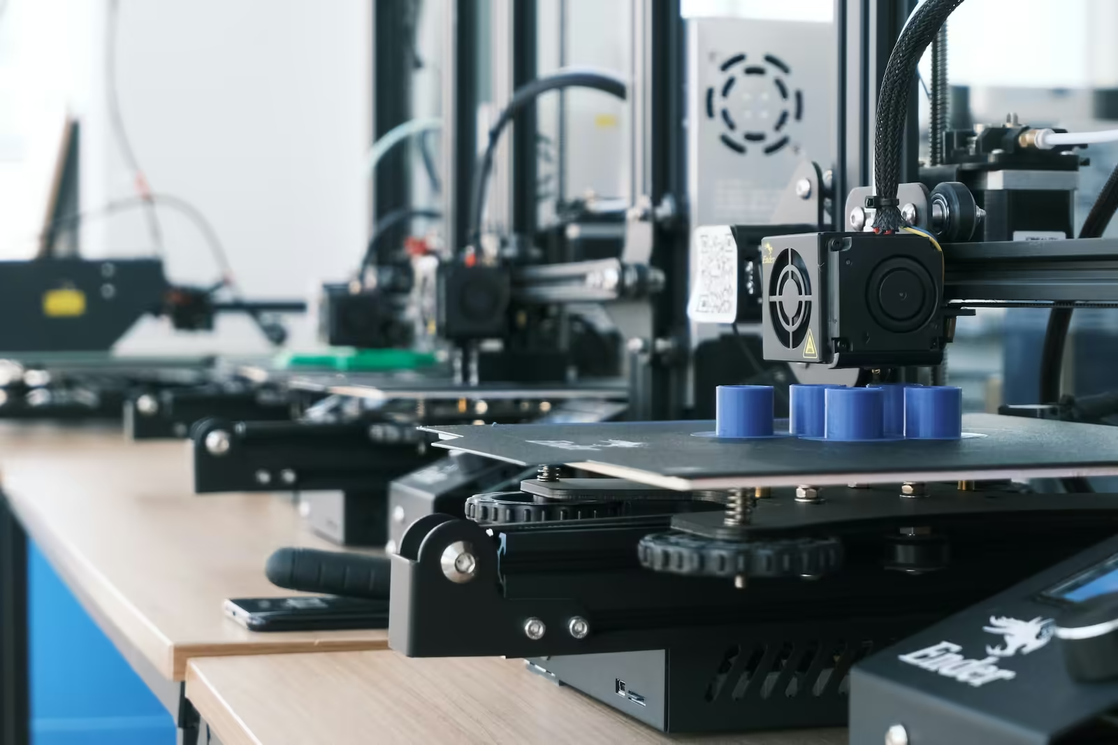
Plasma Treatment for Enhanced Polymer Bonding
In today's fast-evolving industries, from automotive to biomedical devices, the demand for strong, durable, and reliable polymer bonding...
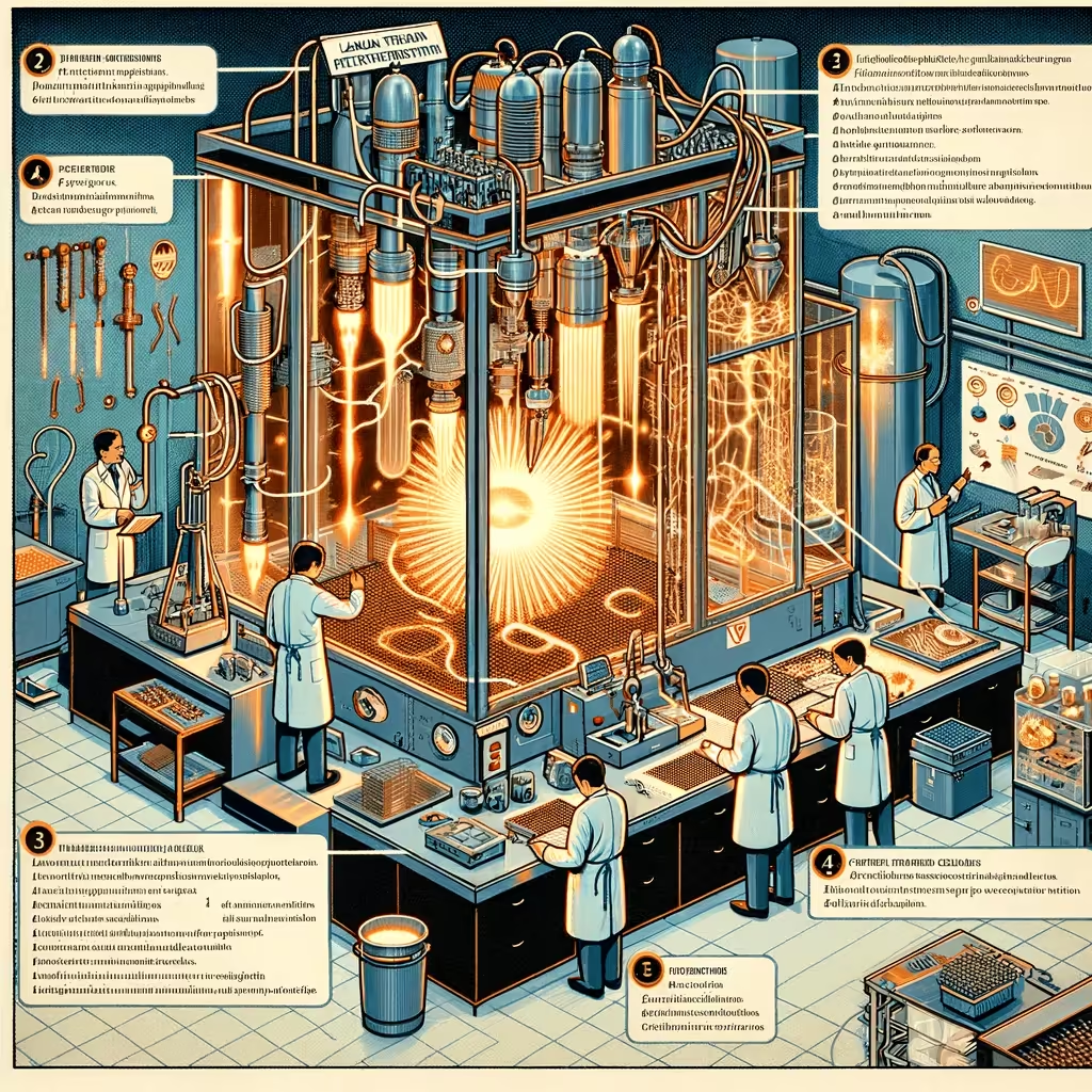
Advanced Plasma Techniques: Transforming Industrial Applications
Plasma, often known as the fourth state of matter, has become a game-changer across numerous industries, enabling innovations that...
No articles match your search. Try a different keyword or tag.