

Plasma Cleaning for Electronics Manufacturing
Flux residue, oxidised pins and low-energy solder mask are invisible on inspection and directly responsible for shorts, coating failures and lifted wire bonds. Vacuum plasma cleaning removes them before assembly.
A PCB doesn't fail because of a bad component — it fails because of what's sitting on the surface underneath a solder joint, a conformal coating, or a wire bond that was never quite clean enough to hold. Flux residue left over from reflow, oxidation on a connector pin, or a low-surface-energy solder mask are all invisible at visual inspection and all directly responsible for the failures that show up as intermittent shorts, coating delamination or a wire bond that lifts under a pull test.
The problem: contamination that hides at PCB scale
Reflow and wave soldering leave flux and rosin residues on the board that reduce insulation resistance and can cause electrical shorts if not removed. Semiconductor wafers, connectors and IC packages arriving for assembly need surfaces clean enough for reliable wire bonding and epoxy application — organic residues from prior process steps get in the way of both. Conformal coating, applied specifically to protect boards from moisture, dust and chemicals, only works if it wets and adheres uniformly; a contaminated or low-energy surface leaves pinholes and thin spots that defeat the coating's purpose before the board ever leaves the factory.
Miniaturisation compounds the problem. Traditional solvent wiping or spraying is a line-of-sight process — it can't reliably reach under low-clearance components, into fine-pitch connector gaps, or between closely spaced pins on a modern board. A cleaning method that depends on physically contacting or flooding the surface leaves exactly the geometries that matter most untouched.
Where vacuum plasma cleaning fits
Vacuum plasma treatment is a gas-phase process, not a line-of-sight one — the ionised gas fills the chamber and reaches under components, into vias and between fine-pitch pins in a way a wipe or spray cannot. Argon physically sputters away oxide layers and inorganic contamination without altering the surface chemistry beneath; oxygen chemically oxidises flux, rosin and machining oils into volatile byproducts that are pumped away rather than smeared around; hydrogen reduces stubborn metal oxides on connector and lead-frame surfaces back to a bare, conductive state. The process is entirely dry — no solvent residue, no ionic contamination, nothing to interfere with high-impedance circuitry downstream.
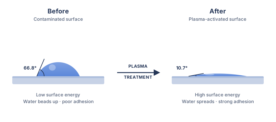
The same plasma exposure does two things at once: it etches the surface at a microscopic level, increasing roughness and giving an epoxy or underfill more area to mechanically key into, while simultaneously raising the surface's chemical energy so the material wets and spreads uniformly instead of beading. That combination is why plasma preparation shows up ahead of conformal coating, epoxy bonding and wire bonding alike — the same treatment step serves adhesion problems that look different but come from the same root cause.
Where it sits in the assembly process
- Wire bonding preparation — strips oxidation and organics from bond pads, lead frames and connector interfaces, improving bond integrity and pull/shear strength.
- Conformal coating preparation — removes flux and organic residues and raises surface energy so the coating spreads uniformly, closing off the pinholes that let moisture and contaminants through.
- Epoxy bonding and underfill — etches and chemically activates the surface around die and BGA packages, improving both the mechanical interlocking and chemical bond strength of the epoxy.
- Package molding — activates lead frame and substrate surfaces ahead of the mould compound so the seal holds against moisture and dust ingress over the product's life.
- PCB and connector cleaning — strips post-reflow flux and rosin residue, restoring insulation resistance and eliminating a common source of intermittent shorts.
Matching the system to the line
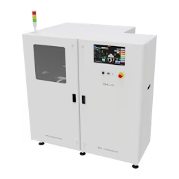
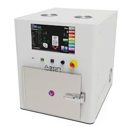
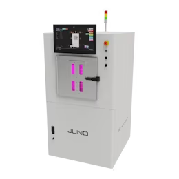
Aeon is a table-top batch system suited to lab qualification and lower-volume manufacturing — PCB, BGA and module cleaning ahead of wire bonding, underfill or conformal coating without committing to a full inline footprint. QML-CI is the inline platform for 24/7 continuous production, in service on module and PCB lines since 2015, with a conveyor-indexer that loads and unloads the chamber in one motion and traceability options for MES integration. Juno is the batch system for mixed part shapes: its reconfigurable shelf layout adapts to almost any component geometry, so a run of varied boards, modules and assemblies shares one chamber without a dedicated carrier.
Verifying the result
Contact-angle measurement before and after treatment is the fastest way to confirm a plasma cycle actually raised surface energy rather than merely running; a result drifting back toward the untreated baseline is an early sign of a fouled chamber or an exhausted gas line. Downstream, correlating plasma cycle data against insulation-resistance testing, conformal-coating adhesion checks and wire-bond pull/shear results closes the loop between the surface-prep step and the failure modes it exists to prevent.
Recommended systems
Related applications
Related articles
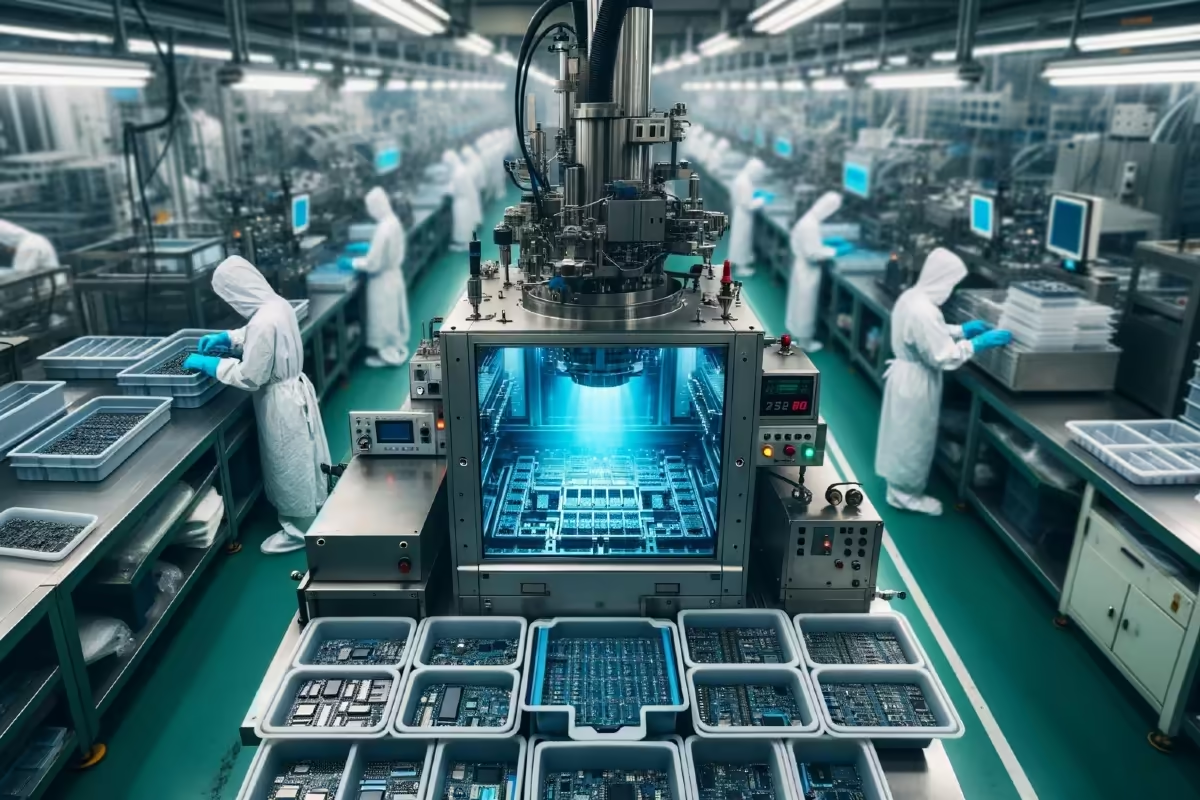
Plasma Cleaning in the Electronics Industry
Plasma cleaning is a dry & environmentally friendly technique answering the needs of the electronics industry.
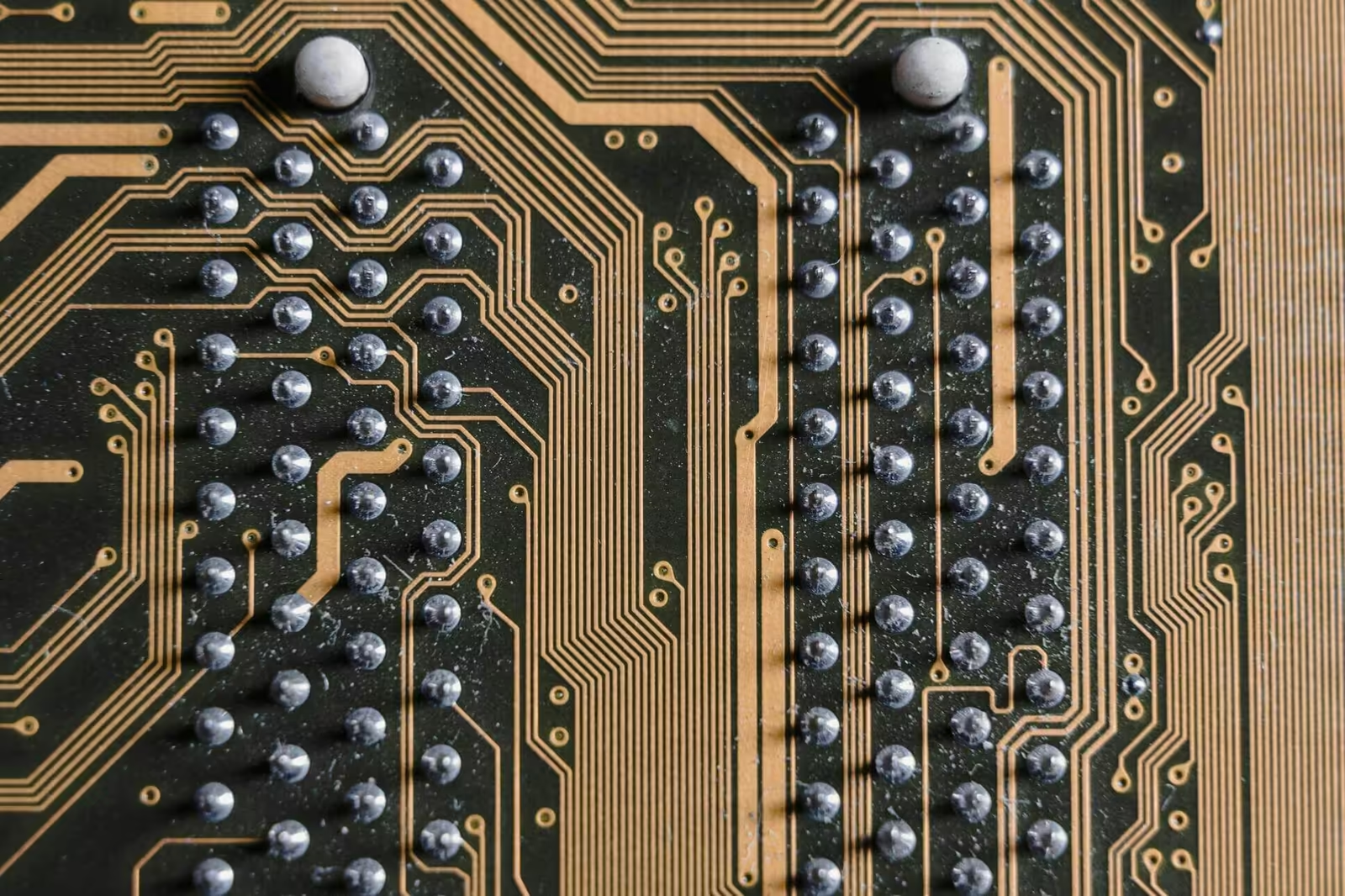
The Uses of Plasma Cleaning Prior To Conformal Coating
Historically, surface cleaning and adhesion promotion in circuit boards were managed using wet chemical treatments or by applying...
The Uses of Plasma Cleaning Prior To Epoxy Bonding
Plasma treatment is a critical step in ensuring the efficacy and durability of epoxy bonds in various industrial applications. Its...
Frequently asked questions
Why does flux residue matter if the board passes electrical test at the end of the line?
Flux and rosin residue reduces insulation resistance gradually; a board can pass initial test and still develop intermittent shorts or leakage current in the field as residue absorbs moisture over time.
Can plasma cleaning reach under low-clearance components and fine-pitch connectors?
Yes — plasma is a gas-phase process, not line-of-sight, so it fills the chamber and reaches under components and between closely spaced pins in a way solvent wiping or spraying cannot.
Does the same plasma step work for conformal coating prep and wire bonding prep?
Both problems come from the same root cause — low surface energy and organic contamination — so the same argon/oxygen/hydrogen plasma chemistry addresses both, with process parameters (gas, power, time) adjusted per application.
When should we use Juno instead of Aeon or QML-CI?
Juno is the batch system for mixed part shapes — its reconfigurable shelves adapt to almost any component geometry, so varied boards, modules and assemblies share one chamber. Choose it over Aeon when a batch outgrows a table-top footprint, and over QML-CI when parts don't suit a continuous inline carrier.
How do we verify the plasma step is working on a production PCB line?
Track contact angle before and after treatment as a wettability check, and correlate plasma cycle data against insulation-resistance testing, coating adhesion checks and wire-bond pull/shear results.