

Semiconductor manufacturing leaves little room for surface contamination. Organic residues, inorganic contaminants, and surface oxides can interfere with bonding and other downstream processes, even when they are too small to be detected through visual inspection.
Plasma cleaning uses ionized gas to remove contamination and modify a surface, helping prepare semiconductor components for processes where cleanliness and adhesion are critical.
But where does plasma cleaning fit into semiconductor manufacturing, and how can it help address problems such as poor bondability and NSOP?
This guide looks at how the process works, where it is used, and the plasma system options available for semiconductor production.
Why Semiconductor Surfaces Need Plasma Cleaning
A semiconductor surface can look clean and still create problems further down the manufacturing line. Contamination introduced during manufacturing, variation in process conditions, or cross-contamination from other process steps can leave residues on dies, lead frames, and bonding pads. These contaminants may be too small to identify through visual inspection, yet they can interfere with adhesion and surface preparation.
Organic contamination and residues left behind by processes such as die attach or snap curing can create a barrier between the surface and the material that needs to bond to it. When the surface is not adequately prepared, the result can be inconsistent bonding and reduced package yield.
Surface oxides present another challenge. In some applications, oxides on a bonding pad can contribute directly to NSOP (Non-Stick on Pad), where the wire bond fails to adhere to the die's pad surface. Plasma cleaning can address these oxide layers through physical and/or chemical interaction, helping restore the surface condition needed for reliable bonding.
For semiconductor manufacturers, the goal is therefore not simply to make a component look clean. It is to control the surface condition before a critical process such as wire bonding, molding, die attach, or underfill.
Plasma cleaning provides a controlled way to remove contamination and modify the surface so it is better prepared for the next manufacturing step.
How the Plasma Cleaning Process Works
Plasma cleaning is a controlled process designed to remove microscopic contamination while preparing a semiconductor surface for the next manufacturing step. The exact result depends on the gas used and the process parameters selected for the application.
The Part Enters a Controlled Chamber
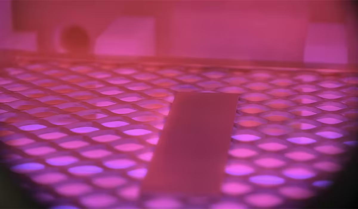
The component is placed inside a vacuum chamber, where the environment can be carefully controlled throughout the treatment. Once the chamber is prepared, the selected process gas is introduced and the pressure, power, gas flow, and treatment time are adjusted to suit the application.
The Process Gas Becomes Plasma
The process gas is energized using an external energy source, causing it to become ionized and form plasma. The resulting plasma contains reactive species that can interact with the surface and its contaminants.
The process gas is selected according to the type of contamination or surface condition being addressed. Argon, for example, can be used to remove organic residues from semiconductor components. Where surface oxides are the concern, an Ar/H2 plasma can be used instead, with the hydrogen radicals reacting chemically with the metal oxides.
Reactive Species Clean and Activate the Surface
Once the plasma interacts with the component, reactive species break down contaminants and residues on the surface. These materials can then be removed from the chamber, leaving the surface clean.
The process can also activate the surface by increasing its surface energy, making it more receptive to bonding and adhesion. In oxide-sensitive applications, Ar/H2 plasma can provide more effective and faster oxide removal than pure argon ion bombardment, helping restore the surface condition needed for reliable wire bonding.
The result is not simply a surface that looks clean. It is a controlled surface condition designed to support the specific manufacturing process that follows.
NSOP: The Failure Plasma Cleaning Prevents
One of the problems plasma cleaning can help address in semiconductor wire bonding is NSOP (Non-Stick on Pad). NSOP occurs when the wire bonder detects that a bond has been created unsuccessfully because the wire has not adhered to the die's pad surface.
A 2012 study by Amy Ang, L.C. Ying, and A. Xavier of Infineon Technologies examined NSOP on a gold-coated palladium bonding pad developed for copper wire bonding. While the pad design offered improved hardness and helped address silicon cratering, the assembly experienced a high rate of NSOP associated mainly with surface oxides.
The researchers investigated whether plasma cleaning could reduce the oxide-related problem. They compared pure argon plasma with an Ar/H2 plasma, where hydrogen radicals can react chemically with metal oxides. The results showed a significant reduction in the NSOP rate with Ar/H2 compared with argon alone, with the treatment also contributing to higher wire bonding yield.
The study illustrates why identifying the condition affecting a bonding surface matters. Where surface oxides are contributing to NSOP, selecting a plasma process suited to that specific surface condition can help improve bondability and wire bonding yield.
Where Plasma Cleaning is Used in Semiconductor Manufacturing
Plasma cleaning can be used at several points in semiconductor assembly and packaging where surface contamination or poor adhesion can affect the next process. The specific purpose varies by application, but the underlying goal is the same: prepare the surface for more reliable processing.
Wire Bonding Preparation
Before wire bonding, plasma cleaning can prepare dies, lead frames, and bonding pads by removing organic contaminants and surface oxides. A cleaner, properly prepared surface can improve bondability and help reduce NSOP failures where contamination or oxides are contributing to poor adhesion.
Die Attach and Underfill
Plasma treatment can also be used to prepare surfaces for adhesives used in die attach and underfill processes. By cleaning and modifying the surface, plasma treatment can improve adhesion between the materials and help address issues such as voiding and delamination.
Lead Frame Cleaning
Lead frames can accumulate organic residues and other contamination during manufacturing and assembly. Plasma cleaning provides a dry method of preparing these surfaces, helping improve bondability and providing a more consistent surface for subsequent processes.
Flip Chip and Wafer-Level Packaging
Plasma cleaning can also support flip-chip assembly and wafer-level packaging (WLP) by preparing surfaces before bonding or other downstream processes. In these applications, surface cleanliness and condition can affect adhesion and interconnect reliability, making controlled surface preparation an important part of the process.
Types of Plasma Systems for Semiconductor Lines
The right plasma system depends on how components move through production and the level of automation required. Batch and in-line systems support different production environments, while direct plasma is a configuration used when components are particularly sensitive to RF exposure.
Batch Plasma Systems
Batch plasma systems process components together inside a vacuum chamber rather than treating them continuously on a production line. This makes them well suited to applications such as lead frame cleaning and manufacturing environments where different product types or volumes need to be accommodated. Components can be manually or semi-automatically loaded, allowing greater flexibility when production requirements change.
In-Line Plasma Systems
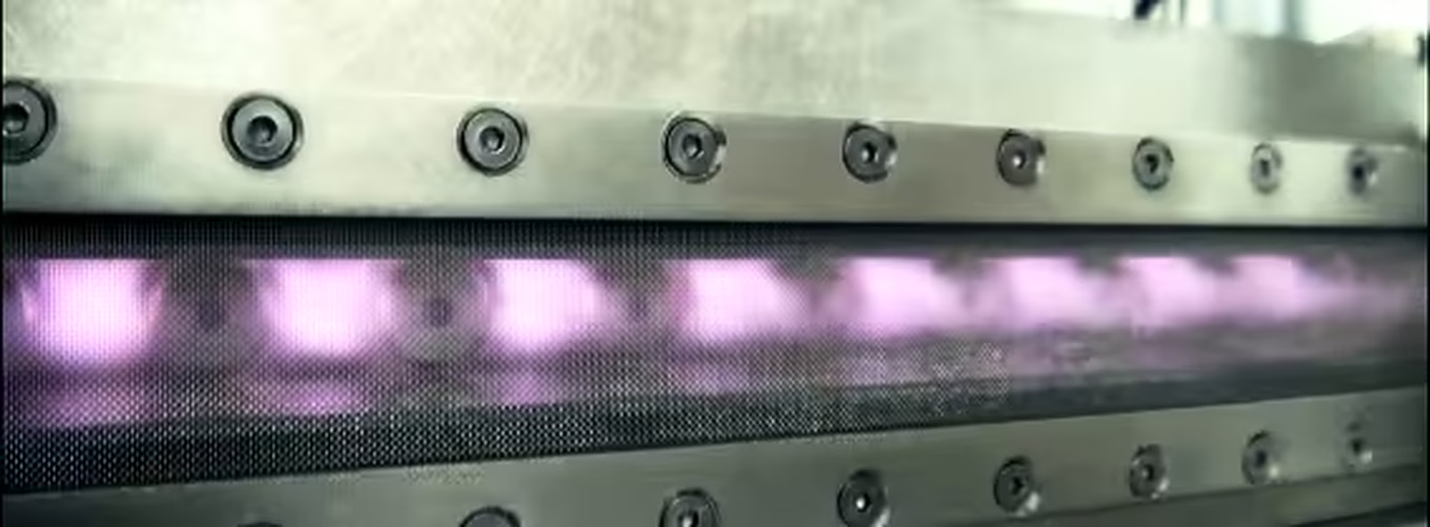
In-line plasma systems integrate plasma treatment directly into the production line, allowing components to be treated as they move through the manufacturing process. Automated handling supports higher-throughput production and reduces the need for manual intervention.
These systems are particularly suited to high-volume manufacturing environments with consistent production workflows.
Direct Plasma
Direct plasma configurations are designed for applications where components are susceptible to damage from direct RF contact. In this setup, the electrode is positioned above the component rather than making direct contact with it. This allows sensitive semiconductor components to undergo controlled plasma treatment while reducing direct RF exposure.
Where Plasma Cleaning Fits in Broader Semiconductor Processing
Plasma cleaning is one part of a broader range of plasma processes used in semiconductor manufacturing, alongside deposition, etching, and doping. While these processes serve different purposes within semiconductor production, cleaning focuses on preparing surfaces by removing contamination and modifying surface conditions before critical downstream steps.
For a deeper look at how plasma is used to remove material with precision, see our guide to plasma etching.
Ready to Improve Your Semiconductor Cleaning Process?
The right plasma treatment depends on the contamination, surface condition, component, and manufacturing process involved. SCI Plasma can help you determine whether plasma cleaning is suitable for your application and identify the right system and process parameters for your production requirements.
Contact SCI Plasma to discuss your semiconductor cleaning requirements.
FAQs
What gas is used in semiconductor plasma cleaning?
Argon is commonly used for cleaning organic residues from semiconductor components. Hydrogen can be used for oxide removal, particularly on oxide-sensitive surfaces. Oxygen can cause unwanted oxidation if it is not properly controlled.
Can plasma damage my device?
Plasma can damage sensitive components if the process is poorly configured or incorrectly tuned. However, parameters such as gas flow, power, pressure, and treatment duration can be controlled to suit the application. Direct plasma configurations can also minimize direct RF contact with sensitive parts.
Is plasma better than wet cleaning for semiconductors?
Plasma cleaning provides a dry, residue-free alternative to wet cleaning and avoids the use of wet chemicals. Its process parameters can also be tightly controlled, making it well suited to semiconductor applications where surface cleanliness and process consistency are critical.
What causes NSOP?
NSOP (Non-Stick on Pad) occurs when the wire bonder detects that a bond has been created unsuccessfully because the wire has not adhered to the die pad. Manufacturing issues, process variation, and cross-contamination can contribute to NSOP. Surface oxides and organic contamination can also interfere with adhesion, which is why plasma cleaning may be used to prepare bonding surfaces.